
E3 Mixed Signal Blog #3 - Schematic Level Design Considerations
/Mixed-Signal Schematic Design
Last time we went over what we felt made mixed-signal PCB design more challenging than a purely analog or purely digital PCB design, now that we have bounded the topic we want to get into some things that us, as designers, can do at the schematic stage of a design convey the intent of our design more clear to those who might inherit the work later on in the product's life.
The purpose of the schematic...
In order to really understand what we are getting at in this blog post we all must (for the purpose of this blog at least) have a common understanding of what the purpose of a schematic is. Or perhaps a better way to put it is: what do we want the schematic to be, and to do for us as we document our design intent.
Convey the functionality
Far and away the most important thing a schematic should do is clearly convey the functionality of your design. If someone can't pick up the schematic and know (at a moderately high level) what the design is supposed to do, and how it is supposed to do it, you have not really done your job as the designer.
One great way to do this is with a first sheet block diagram, showing how the various bits and pieces of your design interact together from a basic connectivity level. Here is a great example from a Terasic board, the DE0-Nano-SoC. Note how there is just enough detail to let you know how things are connected, what is on the board, and how it all connects together. A really great example to learn from.

Source: www.terasic.com
Convey unique information, or special design specific information
What we mean here is that you must convey design specific details in the schematic, a great example of this we are all probably familiar with is the multiple functions on a microprocessor.
In other words, if you are hooking up a microprocessor's GPIO pin as a GPIO, name the connection accordingly! If you are using a GPIO pin as part of an I2C bus, name the connection appropriately! Maybe 'I2C-SDA' for example, instead of just 'GPIO16'
Some of this can be made easier from the schematic symbol creation stage, by putting in all of the possible functions of each pin. Yes, this takes time, but it also makes for a more clear schematic!
Another great way to do this is to enrich your schematic with extra text, pictures and diagrams! Adding key information to your schematic is always a good thing, even if it means using an additional sheet (or two or three) to do so.
A couple of examples of this are shown below, from an E3 Designers schematic. In one example we are showing the configuration mode that an Ethernet PHY is biased into, and in the other we are showing the required switch states for a multiple input range analog front end. By having this information on the schematic you will save yourself, and your colleagues time and make the intent clear to anyone reading it.
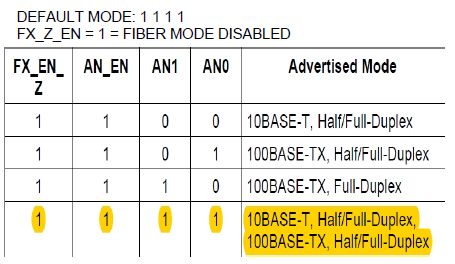
Source: E3 DESIGNERS
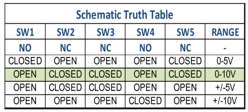
SOURCE: E3 DESIGNERS
Mixed-signal schematic information...
OK, all well and good right? But what does this mean for a mixed-signal PCB design? What kind of information is important to convey especially in a mixed-signal design? Glad you asked...
Multiple GND/return nets...
Sometimes as a designer you will use multiple GND/Return nets in your design. Maybe you have isolated circuitry, sensitive thermocouple conditioning circuitry, high power switch mode power supply returns or localized PLL power and return nets.
If this is something you find yourself doing in your designs make it easy for yourself (and the rest of us!) and name those return nets appropriately! Is it more clear to use a different symbol? Maybe. Is it even more clear to use a different symbol and a unique name like 'PLL-RTN', 'PGND', 'AGND' or 'ISO-GND'? Absolutely.
What's the point though? All that extra work typing, naming the nets...who has the time? Most seasoned engineers will appreciate this, it tells them that the return plane was isolated or cut for a reason, and for a good reason at that. It tells the engineers that will use the schematic that you were paying attention to the details! And it will convey that the multiple return nets were used for a reason, not just because you did so on a whim. It conveys that those nets are intended to serve specific functions, and to help separate circuit return paths - which is sometimes very important in mixed signal designs.
Multiple branches from a power net...
As you may often use multiple power return paths in your design, you may also have to use multiple power supply paths in your design. Sometimes, these paths are not different voltage levels, but may simply be high-frequency isolated from a bulk supply on your circuit. A great example of this would be on a highly integrated DSP, which has internal ADC and DAC devices.
You may want to save board space and cost by using the same VCC supply as a reference voltage for these converters - and that's something that designers often do. But it can get confusing if you don't name those VCC nets clearly.
As an example:
2V5
2V5-1
2V5-2
2V5-3
When you are doing your schematic, sure, you might be able to keep track of things this way, but it can get out of hand very quickly. When you get to the PCB layout, forget about it, you'll be spinning in circles trying to keep track of that naming "convention". Contrast that, with this:
2V5
2V5-ADC-VREF
2V5-DAC-VREF
2V5-PLL
We'll leave it to you to decide which one is more clear, and conveys intent more effectively.
Decoupling capacitors...
Sometimes on a schematic sheet, it can be difficult to place capacitors at each pin - even though that is what you want done on the layout. This is where the use of some simple text notes can make a big difference and be a big help to whoever is doing the PCB layout. It can be as simple as saying...
'Place (1) 10uF and (1) 0.1uF near each VCC pin'
...near a group of 40 capacitors intended for 20 pins of an FPGA
Decoupling in a mixed signal design can be tricky, and the more clear you can convey the design intent you have worked so hard to arrive at the better the end product you will have. Combining notes on the schematic with unique net names and return paths can go a long-way to keeping all the circuits in your design happy and working as you want them to.
Analog circuit notes...
This one is pretty easy to do and can add a lot to the schematic level. If you have spent hours fine tuning an op-amp filter, put a couple of notes there to make it easier to understand the function without getting out a SPICE tool! Some analog filter topologies are complex and unless you live in that world it isn't something most engineers keep at the front of their brain.
Simply writing something like...
'3rd order butterworth LPF, 500kHz -3dB'
...means that engineers who may not be analog gurus, or maybe a more junior engineer can just look at the block and say 'OK, I may not know how to design one of those, but I know what it is supposed to do'. That is more important than many of us know, and something we all often take for granted.
Even just writing the gain of a circuit, and the expected output range can be invaluable for bench debugging done by software engineers or technicians who may not have a lot of design experience. It's useful for us on our own designs! Sometimes there is so much going on that you forget some of the details, that's OK. But write it down, and you will save yourself some pain in the future.
Wrapping it Up
I'm sure by now you are all starting to get the idea - the more useful information you put - the better. It can be for any number of reasons - for software engineers to know how you intended a chip to be biased at start-up or so they know I2C device addresses. It can be for technicians doing bench debugging, so they know what output voltage range you expected to be on certain pins, where certain components were supposed to be placed physically or what a block of circuitry is supposed to do.
In a mixed-signal design this becomes more important than ever because of the complex nature of the beast! Multiple power supply paths, return paths; integrated ASICs, data converters, power converters...the list goes on and on. But the more you can clearly convey in your schematic, the easier life will be for everyone as your design goes from an idea to a product.
In my next column, we'll be taking a look in a little more detail at some things to consider at the PCB layout level for mixed-signal designs. I hope you enjoyed this article and I hope to see you next time. In the meantime, I look forward to receiving your questions and comments.
-Dan